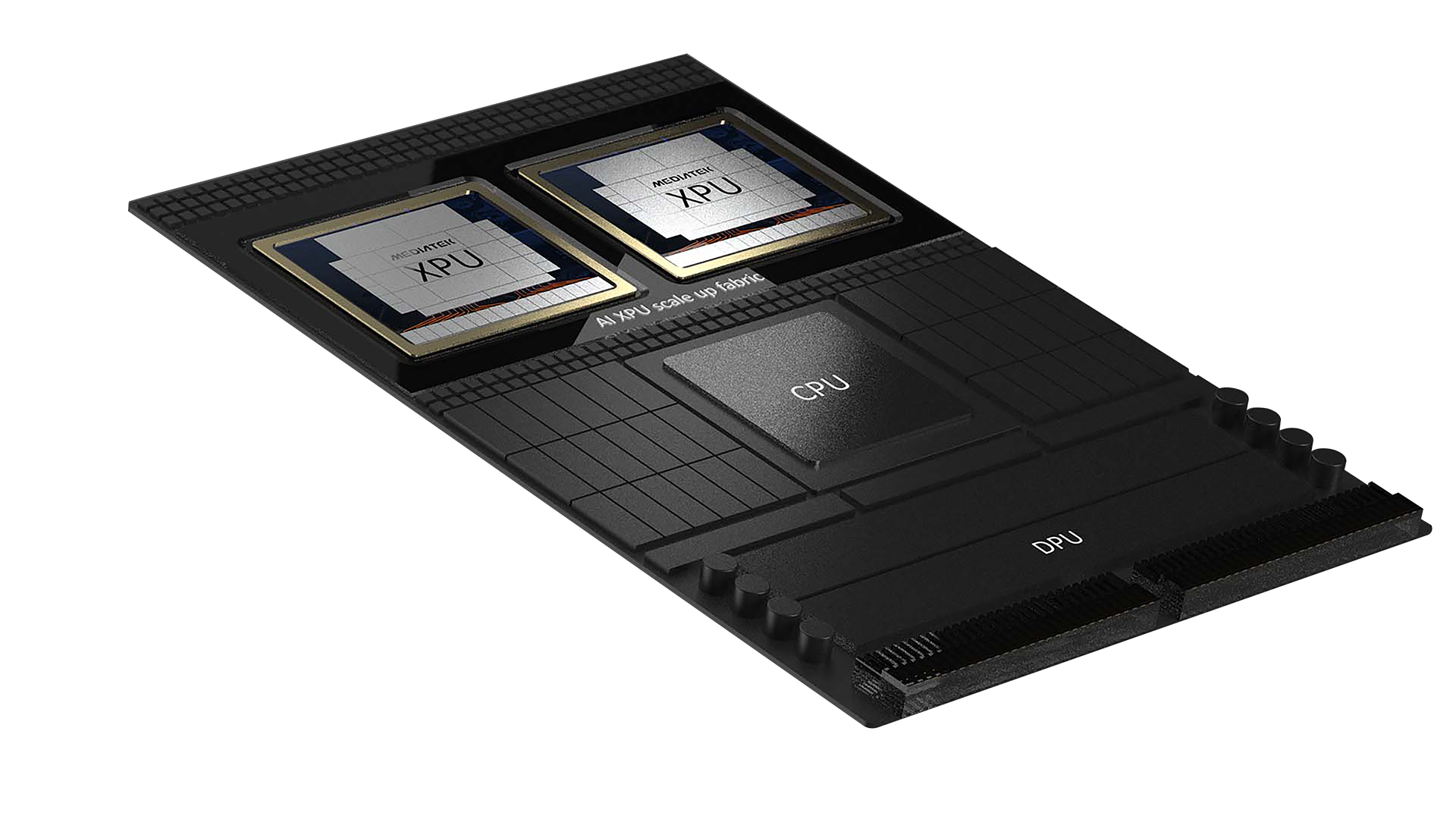
Designed to power next-generation AI use cases, the dedicated compute die delivers the massive parallel processing density required to accelerate complex AI training and low-latency inference workloads at scale.
Why MediaTek for Data Center?
Custom ASIC Design
Whether co-architecting with your IP or designing custom ASICs, we build your perfect XPU.
Custom Proprietary Technology Integration
By integrating your custom proprietary technology, we refine, complete, and deliver the final ASIC design.
Understand Maximizing Process Entitlement to Improve Perf/Watt
Early Node Adoption
MediaTek is at the cutting edge of process technology with 10+ tape-outs on N3, 2+ on N2, and our first A14 test chip taping out later this year.
We lead with mobile - leveraging high volume and scale to optimize yield and process-technology co-optimization, then rapidly apply those learnings to large-scale data center designs. This approach has enabled us to reach advanced nodes for data centers faster than anyone else in the industry.
Design-Technology Co-Optimization (DTCO)
Through Design-Technology Co-Optimization (DTCO), we work directly with leading fabs SOTA process nodes to tweak the process and customize, optimize transistors.
Through Design-Technology Co-Optimization (DTCO), we work directly with leading fabs SOTA process nodes to tweak the process and customize, optimize transistors- extracting every last bit of performance the silicon can deliver.
Whether you're architecting a single ASIC or a fully heterogeneous XPU, we empower any customer to unlock the full potential of the process and turn it into a decisive competitive advantage.
Compute Efficiency Through Lower Voltage Operation
MediaTek's extensive mobile experience gives us a significant head start in applying these learnings to data center chips.
The most impactful way to deliver compute efficiency is running chips at lower voltage. Since power scales cubically with voltage, operating lower has an outsized effect - and with today's fixed power budgets in data centers, this is critical. The real challenge isn't simply running at lower voltage; it's moving the knee of the curve so that performance doesn't drop nonlinearly when you do. This requires deep co-optimization across design, process technology, and circuit architecture. MediaTek's extensive mobile experience - where low-voltage operation is foundational - gives us a significant head start in applying these learnings to data center chips.
Creating the Building Blocks for the XPU
Every XPU begins the same way: with a wafer and a very precise cut. That process — die singulation — divides each wafer into hundreds of identical dies, the raw building blocks that eventually come together as a finished chip.
Every AI Data Center Starts Here
Custom ASICs— designed by MediaTek
Multiple Wafers. Each with Different Functions
AI compute, memory interfaces, interconnects, from individual wafers to complete data center solutions
Die Singulation
Custom ASIC dies ready for advanced packaging
The Compute Die
Purpose-built and engineered for the AI era
Advanced Packaging.
Compute. Memory. I/O.
Unified into one AI powerhouse, built for bandwidth, built for scale.
Advanced Packaging
Packaging is no longer an afterthought because meeting the performance and power-efficiency needs of today can't be achieved without it.
The silicon-packaging co-design is a fundamental part of the modern AI system canvas, where we escape the limits of single die designs and bring heterogeneous components together as one coherent engine.
Advanced Packaging
2.5D
With 2.5D packaging, we can place compute tiles and HBM side-by-side on various silicon interposers, achieving enormous compute performance from a single package.
Spec: <10,000 sq.mm SI
Advanced Packaging
3.5D
3.5D and 3D-style integration introduces vertical die-to-die stacking and more complex integration, minimizing the distances between logic, memory, and I/O, reducing the cost of data movement.
At the same time, heterogeneous integration becomes the key vector of progress. We are bringing together CPUs, XPUs, high-bandwidth memory, high-speed I/O chiplets, and even power and thermal structures together with nanometer precision.
Spec: 10,000-20,000 sq.mm SI
The XPU
Customers can either let MediaTek architect their compute needs from the ground up or integrate their own AI accelerators, logic IP, and microarchitectures into a single, synergistic system.
Compute Die
Designed to power next-generation AI use cases, the dedicated compute die delivers the massive parallel processing density required to accelerate complex AI training and low-latency inference workloads at scale.
Memory Interface Die
Our specialized memory interface dies connect to HBM and other advanced memory technologies, providing the flexibility to meet any bandwidth, capacity, and latency requirements. This enables precise optimization for every class of AI model and deployment scenario.
Memory
Memory dominates AI system BOM costs and power consumption, making performance-per-TCO your toughest challenge. Scaling means balancing capacity, bandwidth, and cost against supply chain realities. MediaTek leads the way with Digital Compute-in-Memory (DCIM) for edge NPUs, performing compute inside the memory array to reduce bandwidth bottlenecks.
Ultra High-Speed IO
We integrate ultra-high-speed I/O and interconnect chiplets, leveraging innovations like co-packaged copper (CPC) for short-reach, high-bandwidth channels. For long-reach connectivity, optical engines (OEs) represent the latest frontier, enabling the transition to co-packaged optics (CPO). These optical engines can be integrated using standard packaging technologies or cutting-edge, interposer-based approaches to maximize integration density.
System-Technology Co-Optimization (STCO)
Building on Design-Technology Co-Optimization (DTCO), System-Technology Co-Optimization (STCO) is required to fully optimize a chip design. This approach leverages advanced platforms such as CoWoS-class and EMIB-class solutions to deliver the perfect balance of performance, density, power, and cost.
The XPU
Customers can either let MediaTek architect their compute needs from the ground up or integrate their own AI accelerators, logic IP, and microarchitectures into a single, synergistic system.
Our specialized memory interface dies connect to HBM and other advanced memory technologies, providing the flexibility to meet any bandwidth, capacity, and latency requirements. This enables precise optimization for every class of AI model and deployment scenario.
Memory dominates AI system BOM costs and power consumption, making performance-per-TCO your toughest challenge. Scaling means balancing capacity, bandwidth, and cost against supply chain realities. MediaTek leads the way with Digital Compute-in-Memory (DCIM) for edge NPUs, performing compute inside the memory array to reduce bandwidth bottlenecks.
We integrate ultra-high-speed I/O and interconnect chiplets, leveraging innovations like co-packaged copper (CPC) for short-reach, high-bandwidth channels. For long-reach connectivity, optical engines (OEs) represent the latest frontier, enabling the transition to co-packaged optics (CPO). These optical engines can be integrated using standard packaging technologies or cutting-edge, interposer-based approaches to maximize integration density.
Building on Design-Technology Co-Optimization (DTCO), System-Technology Co-Optimization (STCO) is required to fully optimize a chip design. This approach leverages advanced platforms such as CoWoS-class and EMIB-class solutions to deliver the perfect balance of performance, density, power, and cost.
State-of-the-art Interconnects
MediaTek delivers a full hierarchy of proprietary interconnect solutions—from on-package die-to-die links (UCIe, MLink) to on-board chip-to-chip connections (SerDes/PCIe, uLED) to long-reach electrical and optical links (SerDes/Ethernet, NPC/CPC, CPO)—each tuned for optimal reach, performance-per-TCO, and performance-per-watt. Built with the entire rack and system in mind, this is custom-scaled performance, not commodity.
On Package
Die-to-die interconnect
Technology
UCIe
MLink
On Board
Chip-to-chip interconnect
Technology
High Speed SerDes (PCIe)
uLED
Off Board
Board-to-board interconnect
Technology
High Speed SerDes (Ethernet)
NVLink Fusion
NPC/CPC Connectors
Co-Package Optics
SCALE-UP
System-to-System
Rack-to-Rack
TECHNOLOGY
Active Optical (Cable)
Active Electrical (Cable)
Co-Packaged Optics
High Speed SerDes (Eth)
Building Blocks of the Data Center
AI Compute System
Co-optimization across three pillars: Compute, Scale-up, and Scale-out Interconnect.
Supports industry standard (UALink, UEC) and proprietary interconnect (NVLink) solution.
Heterogeneous integration to enable new system use-cases with improved performance/TCO.
The Rack
The new unit of compute consumption.
Greater value through hardware/software vertical integration for Cloud AI and enterprise customer.
Power, thermals and reliability dictate the performance.
Effective monetization requires optimization of rack across different usages.
Perf/TCO and Perf/Watt are critical metrics to achieve best-in-class data center efficiency.
In Partnership with MediaTek
NVIDIA NVLink Fusion
As a key participant in the NVLink Fusion ecosystem, MediaTek empowers customers to accelerate their time-to-market with comprehensive rack-level solutions. By seamlessly connecting custom XPUs into NVIDIA's ecosystem via NVLink C2C, our architecture extends from the ASIC Compute Tray and NVSwitch Tray at the rack level, scaling out further through InfiniBand and Ethernet. Leveraging our strong partnership with NVIDIA, we deliver a rare, full-stack data center solution from end to end-an innovation that is already generating strong customer interest.
Next-Gen Active Optical Cable (AOC)
Next-gen Active Optical Cable (AOC) powered by MicroLED light sources and the MOSAIC architecture.
MediaTek and Microsoft proof-of-concept showcases:
- Dramatic power savings
- Extended reach for AI clusters
- Copper-level reliability
- Greater scalability
We're committed to further miniaturization and mass-production readiness for gigawatt-scale AI data centers
Related Posts
FAQs
An XPU is a class of AI accelerator purpose-built to handle the massive parallel compute demands of training and serving large AI models. Unlike a CPU (optimized for general-purpose serial tasks) or a GPU (originally designed for graphics), an XPU is designed from the ground up for AI workloads — maximizing throughput for tensor operations, matrix math, and sparse computations. In a modern AI data center, XPUs sit at the heart of the AI compute system, working alongside CPUs and DPUs (data processing unit is a specialized processor designed to offload networking, storage, and security tasks from a computer's CPU) in a heterogeneous architecture where each processor handles the phase of the AI lifecycle it runs most efficiently. MediaTek designs custom XPUs that are co-optimized with advanced packaging, high-bandwidth memory (HBM), and interconnect as a single unified system.
A custom ASIC (Application-Specific Integrated Circuit) for AI is a chip designed from scratch to match a specific company’s model architecture, workload profile, and infrastructure constraints — rather than relying on off-the-shelf silicon. Hyperscalers and cloud service providers build custom ASICs to gain architectural control, optimize performance per watt and performance per TCO, and avoid the inefficiencies of general-purpose hardware. MediaTek partners with these customers to architect custom ASICs and XPUs end-to-end: from logic die design and memory interface architecture through advanced 2.5D/3.5D packaging and rack-level integration. The result is a workload-specific compute engine that outperforms commodity solutions on the metrics that matter — tokens per watt and tokens per dollar at scale.
An AI compute system is the full hardware stack that trains large AI models and runs high-volume AI inference at scale — it goes well beyond a single chip. At its core is the XPU (AI accelerator), but around it sits a complete fabric: heterogeneous compute (CPUs, DPUs, and XPUs tuned for different workload phases), scale-up interconnect (on-package die-to-die links that keep bandwidth high and energy per bit low), and scale-out interconnect (rack- and data-center-level fabrics built for bandwidth, reach, and efficiency). Memory — HBM, cHBM, LPDDR, SRAM — is co-packaged with compute to reduce data-movement energy. Advanced packaging (2.5D, 3.5D, wafer-level) brings these heterogeneous components together into one coherent engine. MediaTek designs AI compute systems where every element is co-optimized, turning the rack into a strategic asset rather than a collection of parts.
Co-packaged optics (CPO) is a technology that integrates optical engines directly into the chip package — typically on the same silicon interposer or substrate as the compute die and high-bandwidth memory — rather than placing optical transceivers on a separate line card. In AI data centers, where scale-out networking must move enormous volumes of data between racks and rows at low latency and low power, co-packaged optics dramatically reduce the energy per bit and signal loss compared to traditional pluggable optics. As AI clusters scale from hundreds to tens of thousands of XPUs, interconnect power and bandwidth density become first-order constraints, and CPO is emerging as the leading solution. MediaTek integrates co-packaged optics into its AI compute system designs using interposer-based and standard packaging approaches, depending on each customer’s I/O and system-level connectivity needs.
Advanced packaging — including 2.5D and 3.5D integration — enables AI chip designers to escape the physical limits of a single die by combining multiple chiplets (compute dies, memory interface dies, HBM stacks, SerDes, optical engines) into one package that behaves as a unified system. In 2.5D packaging, components are placed side-by-side on a silicon interposer, delivering extreme memory bandwidth inside the package. 3.5D integrations adds vertical stacking, tightening coupling between logic and memory to reduce latency and power. For AI workloads, this matters enormously: memory bandwidth is often the primary bottleneck, and advanced packaging can achieve bandwidth densities that monolithic dies cannot. MediaTek applies design-technology co-optimization (DTCO) and system-technology co-optimization (STCO) across its AI compute systems, with the ambition of achieving 100× improvements in system-level performance per watt and 40× effective increases in reticle-equivalent system size.
AI model training is the computationally intensive process of teaching a large language or multimodal model on massive datasets — it demands extreme memory bandwidth, high sustained throughput, and tolerance for long job durations. AI inference is deploying that trained model to serve real-time predictions, decisions, or generative outputs at scale — it prioritizes low latency, high concurrency, and energy efficiency. Modern AI data centers run both workloads, often on different hardware optimized for each phase. XPUs are tuned for the high-throughput demands of training; DPUs manage network and storage offload; CPUs handle orchestration and control-plane tasks. MediaTek designs heterogeneous AI compute systems where the memory hierarchy, interconnect, and packaging are co-optimized for both training and inference, including differentiated architectures for the prefill and decode stages of inference.
TOPS stands for Trillion Operations Per Second (or Tera Operations Per Second). It measures raw Theoretical throughput, but it ignores power consumption, memory bandwidth constraints, and real workload efficiency — making it a poor proxy for actual AI data center economics. Tokens per watt measures how much useful AI output (tokens generated, predictions served) a system delivers for each watt of power consumed, which directly maps to operating costs and facility capacity. As global data center power consumption climbs and hyperscalers run into grid limits, tokens per watt has become the defining benchmark for evaluating AI accelerators and custom ASICs. MediaTek treats energy as a first-class design constraint across its custom XPU and AI compute system designs — from low-voltage circuit design and compute-in-memory architectures to co-packaged optics and system-level power delivery — to maximize tokens per watt at the rack level.
High Bandwidth Memory (HBM) is stacked DRAM co-packaged with AI accelerators and custom ASICs to provide the extreme memory bandwidth required by large AI model training and inference. As model sizes have grown from billions to trillions of parameters, the memory wall — the gap between compute throughput and memory bandwidth — has become the primary performance constraint in AI systems. HBM addresses this by placing wide-interface memory dies directly on or beside the compute die via advanced 2.5D/3D packaging, achieving bandwidth of multiple terabytes per second per package. MediaTek designs dedicated memory interface dies that connect compute dies to HBM and other memory technologies (cHBM, LPDDR, SRAM), co-optimizing bandwidth, capacity, and latency for each workload class. Looking ahead, emerging technologies like HBF (High Bandwidth Flash) are being designed to enable large-scale inference with unprecedented memory capacity.
Off-the-shelf AI chips are general-purpose accelerators designed to serve many customers across diverse workloads — they are optimized for the median use case, not your specific model architecture, fleet size, or infrastructure constraints. MediaTek’s end-to-end approach means co-designing the custom ASIC or XPU, advanced packaging (2.5D/3.5D), memory hierarchy, high-speed interconnect, co-packaged optics, power delivery, and rack integration as one unified AI compute system — all tailored to a customer’s specific models, power budgets, and TCO targets. This vertical integration allows MediaTek customers to achieve superior performance per TCO and performance per watt versus commodity solutions, while owning their platform architecture for long-term competitive advantage. MediaTek partners with hyperscalers, cloud service providers, and AI platform companies who are making long-term bets on how they train and serve models at scale.
Custom silicon for AI infrastructure refers to chips and systems designed specifically for a company’s AI workloads, rather than purchased as standard commercial products. It spans custom ASICs (application-specific integrated circuits), custom XPUs (accelerator processors), memory interface dies, SerDes chiplets, and optical integration — all architected together as a full AI compute system. Hyperscalers (Google, Meta, Amazon, Microsoft) have led the trend, building custom silicon to optimize training and inference at the scale of millions of GPUs-equivalent compute. Enterprise cloud providers and AI-native companies are increasingly following. The driver is economics: custom silicon can deliver 2–5× better performance per watt and performance per TCO versus off-the-shelf alternatives when designed for a specific model class and deployment environment. MediaTek designs and delivers custom silicon solutions end-to-end — from logic die architecture through advanced packaging, interconnect, and rack integration — in partnership with leading fabs.